Design Strategies for Tab Routing in PCB Manufacturing
Tab routing enhances PCB production efficiency and quality, ideal for complex shapes. It offers cost-effectiveness, flexibility, and protection, crucial for high-precision designs and panelization.
Among the manufacturing of Printed Circuit Boards, one of the crucial techniques employed is the tab routing since it raises the efficiency and quality of production. Design considerations of tab routing are based on how to help engineers and designers achieve the best performance in their projects regarding PCBs. The process has consequences not only on the physical features of the circuit boards but also extends to general production dynamics, hence preferred for many applications. The following details constitute good design for tab routing in conformance with industry standards and practical applications.
Introduction to Tab Routing
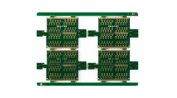
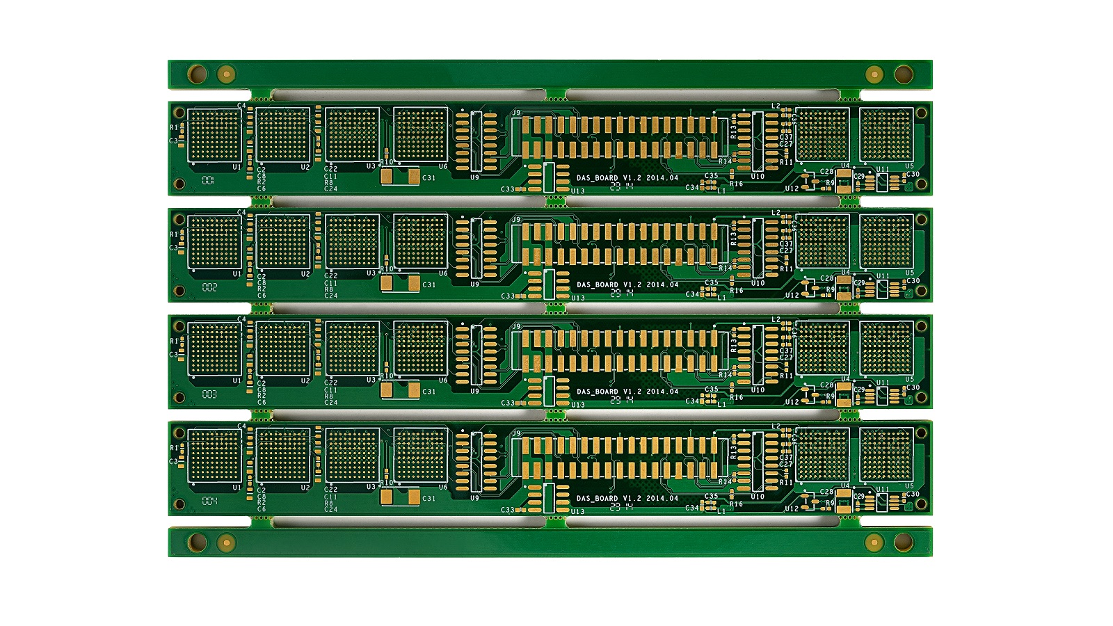
The term tab routing is mostly used interchangeably with terms such as tab route or tab routed PCB, defining a panelization technique where multiple boards are put together into one panel. This may include identical boards or mixed designs in one array. It accommodates batch processing, thereby decreasing the manufacturing cost and increasing the speed of production by adopting efficient panelization practices. It is done by routing the tabs that connect the individual boards. This makes tab routing particularly valuable in the case of non-rectangular PCBs and high-precision designs.
This again talks a lot about the flexibility in the operations of tab routing, as it allows boards to be made in one united panel, yet still provide easy separation. Besides easing production logistics, this process contributes a lot towards strengthening the structure of the boards through many stages of manufacturing and assembly.
Main Design Considerations for Tab Routing
Tab Placement and Size
Tabs should be strategically placed so that there is enough structural support without undue stress at the break points. A practical guideline for placing five-hole perforated tabs is to space them about 2-3 inches from each other on the board edge. This spacing maintains the integrity of the board edges in their assembled and depaneled states.
Clearance
Adequate clearance is very necessary to avoid mechanical and electrical damage. One should keep a distance of at least 1/8 inch from the tabs to adjacent traces and components. In the case of more sensitive components, such as surface-mounted ceramic multilayer chip capacitors, the minimum clearance distance is at least 1/4 inch. The aforementioned precautions will avoid damage due to tab breaking and other assembly stages.
Perforations and Knockouts
Perforations or mouse bites enable every board to be removed easily from a panel. These must not be centered directly on the tabs so as not to have board protrusions. They should be placed near the edge of the PCB or on either side of the tabs, between two PCBs.
Knockouts are useful, especially in designs containing large holes. Wave solder stability is maintained without the possibility of sagging in the center of large arrays.
Edge Components Handling
Tab routing has an advantage compared to v-scoring in supporting PCBs with edge-hanging components. It is important not to have the tabs too close to such components to avoid overlap, which may make separation cumbersome and also cause damage to sensitive parts.
Router Path and Tab Width
A 2mm router bit is normally used, and the spacing between the boards must be at least 2mm. Tab width shall be considered of the order of 3mm +/-0.25mm, while the position tolerances should be +/- 0.5mm. This is the accuracy required to have a clean breakout without compromising board structure.
Breakout Process
Proper handling is required during depaneling. Machine-assisted depaneling, such as by a depaneling router, is advised for thicker boards that might be difficult to manually separate without causing potential damage. Thinner, more flexible boards work great using manual methods with wide-nose pliers, bending the tab both ways until it breaks cleanly along the designed break line.
V-Score vs. Tab Routing
Which one to choose between v-scoring and tab routing depends on the various board design requirements. V-scoring is ideal for rectangular boards because there is less material waste and faster processing. On the other hand, if complex shapes have to be routed or if quality edging and component clearance from the edge are to be considered, tab routing is the method of choice. While tab routing leaves small rough laminate nubs, these can be smoothened down, thus allowing a clean finish post-routing.
Tab Routing Default Specifications
Where customers have specific instructions, apply the default specifications for the panels. It is mandatory that tabs be at least 9 mm away from the corners and key datum points of every board to prevent stress concentrations that can lead to damage. Consider keeping the alignment of tabs consistent in the X-Y axis for consistency in the break lines.
Benefits of PCB Panelization
Besides enabling the manufacture of boards in smaller lots, panelization enhances efficiency in production through tab routing. The following are the advantages of the technique:
Cost-Effectiveness: Panelization provides an opportunity to handle boards parallel to each other, reducing manufacturing time and cost in that particular case. This is very helpful at the prototyping stage when several designs need to be tried economically.
Protection Enhanced: The panelized format protects the boards against mechanical stress and environmental vibrations at the time of manufacturing.
Manufacturing Flexibility: Incredibly, engineers can apply new board constructions to conventional fabrication processes, greatly increasing the ability to innovate with marginal additional cost.
PCB Breakout Guidelines
PCB breakout must be carefully controlled to maintain board integrity. To achieve a blackout that minimizes problems in breakout, make consideration for
Manual Breakout: When manually breaking tabs, it is very important to use tools like wide-nose pliers to properly bend the tabs along the break lines until an effective clean separation is realized.
Machine-Assisted Breakout: Depaneling routers ensure safe and efficient separation for thick boards.
V-Score Breakout: You'll need specific depaneling machines with wheel cutters that separate panels very effectively. The edges are going to be a little rougher as compared to routed boards, yet functionally acceptable.
Conclusion
Tab routing is a very versatile and effective method of PCB panelization, in particular for projects with non-linear board shapes or edge-critical components. The tab routing process can go well and give enough structural integrity while making the production process more effective by observing some design principles. In fact, this approach will satisfy not only the short-term need of assembling PCBs but also support general manufacturing objectives concerning flexibility and cost efficiency. In some cases, tab routing may be preferred, while in other cases, alternative methods such as v-scoring may be preferred, depending on the specific demands placed on the board design and application. The goal is always to ensure quality, functioning, and durable PCBs.
Hot Tags:
Contact us

If you can't find what you're looking for, please contact us.
Article

PCB tabs ensure mechanical stability and easy assembly. They facilitate fabrication by retaining panel stiffness, holding boards, and aiding in depaneling, optimizing manufacturing efficiency and quality.

Effective thermal conductivity is crucial in PCB design for heat management. It depends on factors like component size and thermal vias, aiding reliable, efficient electronic operation through modeling and analysis.

PCB panelization consolidates multiple PCBs into a larger board, improving manufacturing efficiency and reducing waste. Techniques include V-scoring and tab-routing. Proper design enhances assembly, testing, and cost-effectiveness.

